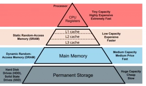
In an era where smartphones process 11 trillion operations daily and AI models require 1 terabyte of active memory, understanding the symbiotic relationship between ROM (Read-Only Memory) and RAM (Random Access Memory) becomes critical. This exploration reveals how these two memory types—one static and eternal, the other dynamic and transient—orchestrate modern computing.
Fundamental Operational Principles
ROM operates as permanent firmware storage:
- Non-volatile data retention (10+ years without power)
- Factory-programmed (Mask ROM) or field-updatable (EEPROM)
- 50-150ns read speeds for boot code execution
RAM serves as temporary workspace:
- Volatile storage requiring constant refresh (64ms cycle)
- 15-25GB/s bandwidth for CPU data pipelines
- 0.1-1ns access times for real-time processing
A smartphone simultaneously uses ROM to store iOS/Android kernels (2-4GB) and RAM for app multitasking (6-16GB).

Physical Architecture & Manufacturing
ROM Chip Structure:
- Floating gate transistors (10nm node)
- NOR/NAND flash configurations
- 3D stacking (128 layers for 1Tb chips)
RAM Chip Design:
- Capacitor-transistor cells (1Xnm DRAM)
- 8Gb dies with TSV (Through-Silicon Via)
- DDR5 interface (6.4Gbps/pin)
Samsung’s 238-layer 3D NAND stores 8TB in postage-stamp size, while SK Hynix’s DDR5 modules achieve 102GB/s transfer rates.
Data Persistence Mechanics
ROM Retention:
- Fowler-Nordheim tunneling for charge trapping
- 100k-1M P/E cycles (Program/Erase)
- 1mV/year charge loss in 3D NAND
RAM Refresh:
- 64ms row refresh interval (8K rows in DDR5)
- 7.8μs CAS latency (CL22 @3200MHz)
- 1.1V operating voltage with error correction
Industrial controllers use ECC RAM to reduce soft errors from 1,000 FIT (Failures in Time) to <10 FIT.
Speed & Latency Comparison
| Parameter | ROM (3D NAND) | RAM (DDR5) |
|---|---|---|
| Read Latency | 50μs | 14ns |
| Write Speed | 700MB/s | 60GB/s |
| Endurance | 3,000 TBW | ∞ (No wear-out) |
| Power Consumption | 3.5W (Active) | 5W/DIMM |
While RAM offers 3,500x faster access, ROM provides 10^6x better data retention.
Application-Specific Implementations
ROM Use Cases:
- UEFI firmware (32-256MB SPI ROM)
- Automotive ECUs (OTA-updatable 1GB NOR)
- Medical device software (Rad-hardened PROM)
RAM Workloads:
- In-memory databases (2TB+ per node)
- GPU frame buffers (24GB GDDR6X)
- AI tensor operations (HBM2e @1.8TB/s)
NVIDIA’s H100 GPU combines 80GB HBM3 (RAM) with 128MB L2 cache (SRAM) for exascale computing.
Evolutionary Trajectories
Next-Gen ROM Tech:
- PLC (5-bit/cell) NAND achieving 200+ layers
- Optane-like 3D XPoint (Phase-Change)
- DNA storage prototypes (1EB/gram density)
Future RAM Innovations:
- MRAM (Magnetoresistive): 10ns non-volatile
- CXL (Compute Express Link): Unified memory
- FeRAM: 10^15 endurance cycles
Intel’s Optane Persistent Memory blurs lines with 512GB modules offering 8μs access times.


Leave a comment