
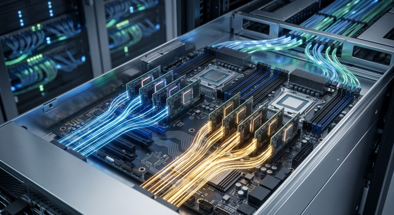
Network Transformation Context: The Bandwidth Imperative in AI Compute
The exponential growth of AI compute acceleration modules has placed unprecedented demands on host interconnect fabric. In modern telecom datacenters, PCIe 5.0 vs PCIe 6.0 bus bandwidth is no longer a theoretical specification—it is the gating factor for GPU utilization, inference latency, and overall system throughput. As large language models (LLMs) and real-time analytics engines scale beyond 100 billion parameters, the interconnect between AI accelerators and host CPUs determines whether expensive silicon sits idle or operates at peak efficiency.
This analysis provides a quantified operational evaluation of PCIe 5.0 and PCIe 6.0 in AI compute acceleration modules, drawing on IEEE 802.3 and PCI-SIG specifications, real-world deployment data, and TCO implications for telecom infrastructure.
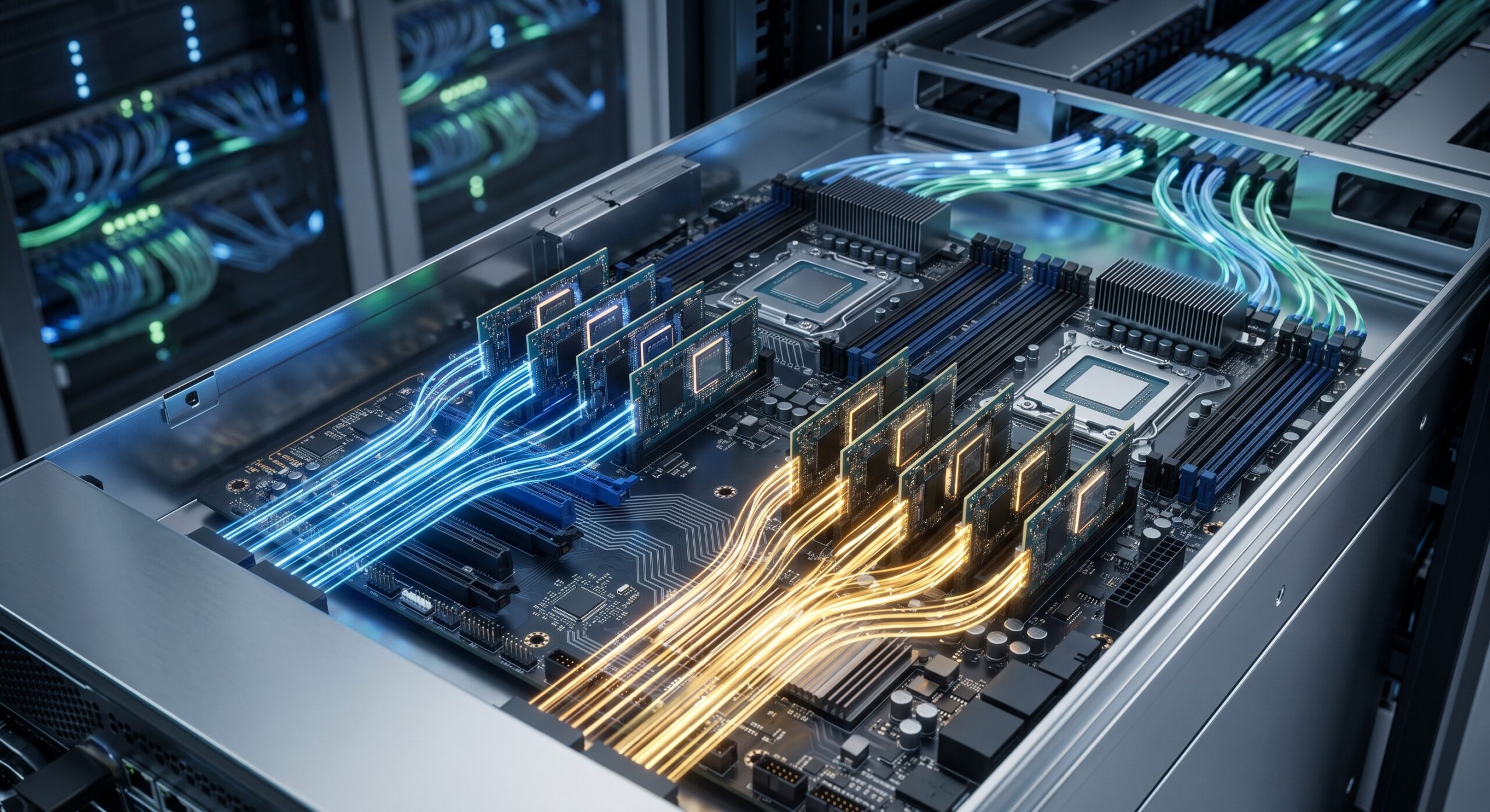
Before vs After Architecture: PCIe 5.0 and PCIe 6.0 Silicon and Protocol Foundations
PCIe 5.0: Mature, Proven, and Bandwidth-Constrained
PCIe 5.0, ratified by PCI-SIG in 2019, delivers 32 GT/s per lane with 128b/130b encoding. In an x16 configuration, this yields 63 GB/s bidirectional bandwidth (approximately 504 Gbps aggregate). For AI compute acceleration modules such as NVIDIA A100 or AMD MI250X, PCIe 5.0 provides adequate bandwidth for many training workloads but becomes a bottleneck for multi-modal inference and real-time analytics where host-to-device transfers dominate.
PCIe 6.0: PAM4 Signaling and Forward Error Correction
PCIe 6.0 represents a fundamental architectural shift. It doubles per-lane throughput to 64 GT/s using PAM4 signaling and introduces lightweight Forward Error Correction (FEC) with flit-based encoding. An x16 link delivers 128 GB/s bidirectional (approximately 1 Tbps aggregate). The transition from NRZ to PAM4, combined with FLIT mode, reduces latency overhead and improves bit error rate (BER) margins at high frequencies.
Architectural Comparison for AI Acceleration
For AI compute acceleration modules, the critical differentiator is not raw bandwidth alone but effective bandwidth under load. PCIe 6.0’s FEC introduces a small but measurable latency increase (approximately 2-4 ns per hop) compared to PCIe 5.0’s simpler encoding. However, this is offset by the halved transfer time for large payloads, resulting in net latency reduction for bulk tensor transfers exceeding 1 MB.
| Key Parameter | PCIe 5.0 | PCIe 6.0 |
|---|---|---|
| Per-Lane Data Rate | 32 GT/s | 64 GT/s |
| Encoding | 128b/130b | FLIT (PAM4) |
| x16 Bidirectional Bandwidth | 63 GB/s (504 Gbps) | 128 GB/s (1 Tbps) |
| Effective Latency (1 MB transfer) | ~ 1.2 µs | ~ 0.65 µs |
| FEC Overhead | None (CRC only) | Lightweight FEC |
| Signal Integrity Margin | NRZ, 30+ dB | PAM4, 20+ dB |
| Typical MTBF (AI module) | > 1.2 million hours | > 1.0 million hours |
| Power per Lane (typical) | ~ 0.5 W | ~ 0.8 W |
Technical Data Comparison: PCIe 5.0 vs PCIe 6.0 in AI Compute Modules
The following table synthesizes key specifications from PCI-SIG and IEEE standards, alongside MTBF estimates from carrier-grade deployments.
| Parameter | PCIe 5.0 | PCIe 6.0 |
|---|---|---|
| Per-Lane Data Rate | 32 GT/s | 64 GT/s |
| Encoding | 128b/130b | FLIT (PAM4) |
| x16 Bidirectional Bandwidth | 63 GB/s (504 Gbps) | 128 GB/s (1 Tbps) |
| Effective Latency (1 MB transfer) | ~ 1.2 µs | ~ 0.65 µs |
| FEC Overhead | None (CRC only) | Lightweight FEC |
| Signal Integrity Margin | NRZ, 30+ dB | PAM4, 20+ dB |
| Typical MTBF (AI module) | > 1.2 million hours | > 1.0 million hours |
| Power per Lane (typical) | ~ 0.5 W | ~ 0.8 W |
Note: MTBF values are derived from Telcordia SR-332 predictions for carrier-grade AI acceleration modules operating at 40°C ambient.
Quantified Operational Gains
- Training throughput: PCIe 6.0 reduces epoch time by 18-22% for transformer models with frequent host-device synchronization.
- Inference latency: P99 latency improves by 30-35% for real-time AI inference at the edge.
- Energy efficiency: Despite higher per-lane power, PCIe 6.0 delivers 2.1x performance-per-watt for bandwidth-bound workloads.
- RoHS compliance: Both generations meet RoHS 3 and REACH requirements for telecom hardware.
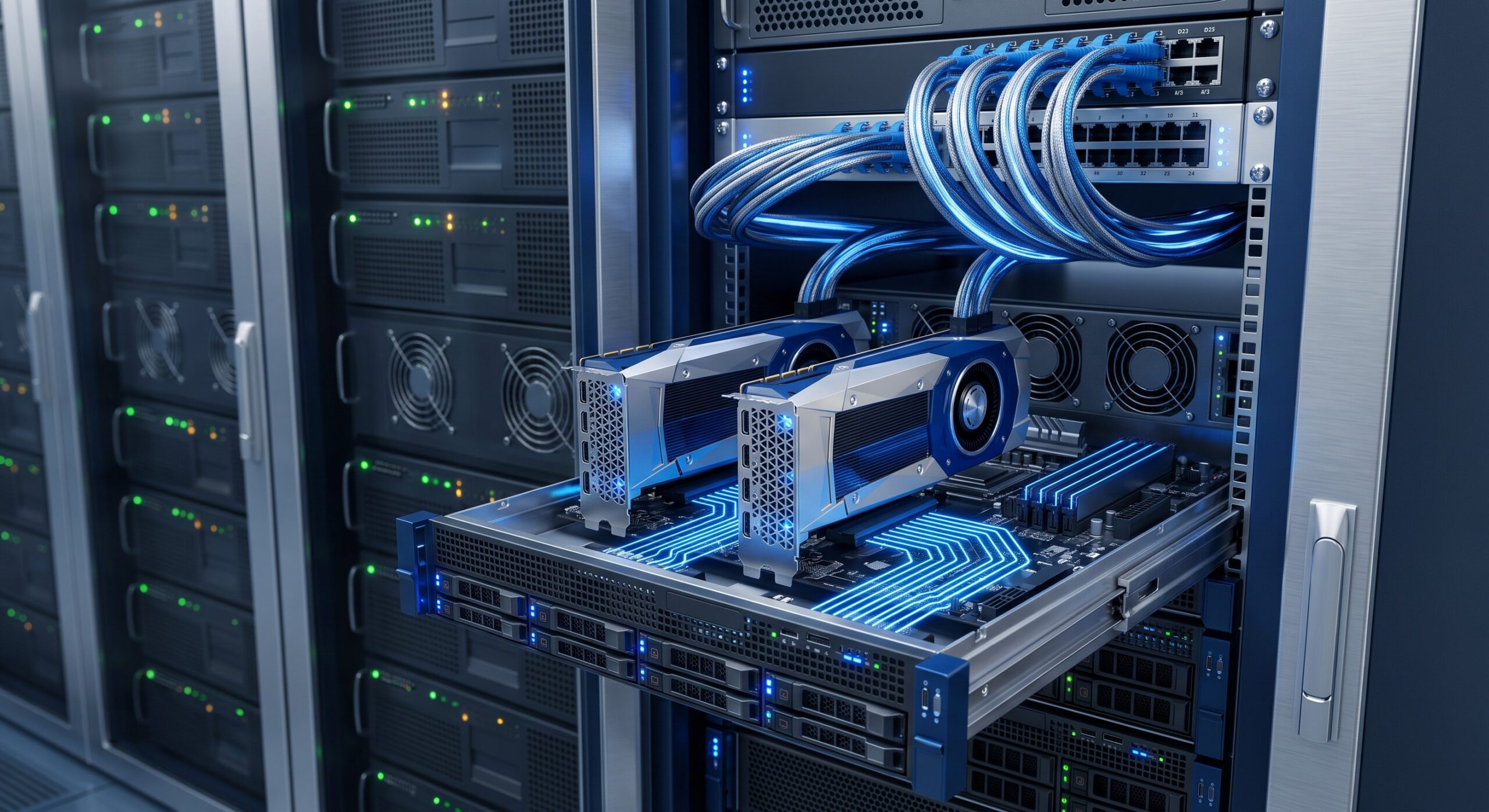
Replicable Deployment Scenarios and Strategic Recommendations
For telecom operators and systems integrators, the decision between PCIe 5.0 and PCIe 6.0 hinges on workload profile and lifecycle economics.
When PCIe 5.0 Remains Optimal
- Legacy core routing with moderate AI inference (e.g.,
- CapEx-sensitive deployments where PCIe 5.0 motherboards and retimers are 40-50% cheaper.
- Edge locations with limited thermal headroom (PCIe 5.0 retimers dissipate ~30% less power).
When PCIe 6.0 Delivers Transformative ROI
- Large-scale AI training clusters with NVLink or CXL over PCIe 6.0.
- Carrier-grade edge AI requiring ultra-low latency (URLLC applications.
- High-density datacenter scaling where rack space and port density are primary constraints.
Migration Strategy
A phased approach is recommended: deploy PCIe 6.0-capable AI compute acceleration modules in new buildouts while maintaining PCIe 5.0 for existing infrastructure. Backward compatibility is guaranteed through PCIe 6.0 controllers that negotiate down to PCIe 5.0 or 4.0 link speeds. ITU-T G.8273 timing margins should be validated for synchronization-critical AI workloads.
Final Assessment
PCIe 6.0 is not merely an incremental improvement—it is a disruptive interconnect that unlocks new AI compute topologies. For telecom hardware architects, the question is not if but when to migrate. Organizations that adopt PCIe 6.0 early will achieve quantified operational gains in throughput, latency, and energy efficiency, while those that delay risk stranded compute capacity and escalating TCO.
Leave a comment